Home › Forums › TinyG › TinyG Support › G28.2 command to auto-level a PCB?
Tagged: auto-level, pcb, z-probe
- This topic has 4 replies, 2 voices, and was last updated 12 years ago by
jlauer.
-
AuthorPosts
-
July 1, 2014 at 11:49 am #6311
jlauer
MemberHi Alden,
I’m wondering if you think using the G28.2 command could be an effective strategy to auto-level a PCB before milling? Or if you think there could be a better approach using TinyG?
PCBs typically have a warpage of 0.1 to 0.2 mm across the board depending on how large the PCB is. One way to combat this is to have a vacuum table to suck the PCB down flat. Most folks don’t have a vacuum table and in many cases vacuum tables kill your ability to drill holes in the PCB.
An alternative technique is to measure the warpage by probing and then adjust the Z positions of the Gcode to compensate for the warpage. On a 40mm x 40mm PCB board you could probe every 2mm to get a good Z offset grid.
If I run a G28.2 command after attaching wires to the PCB and the endmill and then connecting those to the Z Min switch on the TinyG I get the following output from TinyG:
g28.2 z0
{“r”:{“f”:[1,0,9,3334]}}
{“sr”:{“coor”:0,”dist”:1}}
{“qr”:28}
{“qr”:27}
{“sr”:{“vel”:15.21,”mpoz”:-0.008,”stat”:9}}
{“sr”:{“vel”:20.00,”mpoz”:-0.041}}
{“sr”:{“mpoz”:-0.074}}
{“sr”:{“mpoz”:-0.106}}
{“sr”:{“mpoz”:-0.139}}
{“sr”:{“mpoz”:-0.172}}
{“sr”:{“mpoz”:-0.204}}
{“sr”:{“mpoz”:-0.237}}
{“sr”:{“mpoz”:-0.271}}
{“sr”:{“mpoz”:-0.302}}
{“sr”:{“mpoz”:-0.336}}
{“sr”:{“mpoz”:-0.369}}
{“sr”:{“mpoz”:-0.401}}
{“sr”:{“mpoz”:-0.434}}
{“sr”:{“mpoz”:-0.467}}
{“sr”:{“mpoz”:-0.499}}
{“sr”:{“mpoz”:-0.532}}
{“sr”:{“mpoz”:-0.566}}
{“sr”:{“vel”:19.05,”mpoz”:-0.598}}
{“qr”:27}
{“sr”:{“vel”:10.00,”mpoz”:-0.587,”stat”:9}}
{“sr”:{“mpoz”:-0.570}}
{“sr”:{“mpoz”:-0.553}}
{“sr”:{“mpoz”:-0.538}}
{“sr”:{“mpoz”:-0.521}}
{“sr”:{“mpoz”:-0.504}}
{“sr”:{“mpoz”:-0.488}}
{“sr”:{“mpoz”:-0.472}}
{“sr”:{“mpoz”:-0.455}}
{“sr”:{“mpoz”:-0.439}}
{“sr”:{“vel”:2.22,”mpoz”:-0.425}}
{“sr”:{“vel”:0.00,”mpoz”:-0.425,”stat”:3}}
{“qr”:28}
{“sr”:{“mpoz”:0.000,”coor”:1,”dist”:0}}In that output, if I scan it and look for the lowest Z poisition I see “mpoz”:-0.598. That would then be recorded for that probe location. Running this for all grid points I could get the differing values and create the auto-level grid.
The problem is my Z position reference is lost on each probe step because the Z gets set back to 0. So, i could reset it with a G28.3 command, but that seems like it wouldn’t be accurate anymore. I could perhaps look at each probe step as if it’s a relative offset from the last probe step. If I could instead just ask during the G28.2 to NOT reset Z to zero that could solve my problem perhaps. Also, the Z positions given to me by the TinyG may not be the bottom-most Z position when the Z Min switch is hit because the TinyG is only reporting to me every N ms. So, I may be getting decent data, but not perfect data.
Do you think this would work? Do you have any other strategies? One other idea is to just use an Arduino with an independent probe rather than try to coerce the TinyG into doing this for me.
Thanks,
JohnJuly 4, 2014 at 10:28 am #6324flux
MemberHello,
The new G38.2 command available in the Edge firmwares is what you need. Ie:
G38.2 Z-10 F50moves till the A limit switch (I’m not certain about this) connects or till it reaches Z-10, whichever happens first.
This has a few nice features:
1) It doesn’t mess with your offets, so you can still G0 Z0 to move the tool up
2) It returns absolute position so you can use G10 L2 Px commands with it regardless in which coordinate system you are in
3) It works for any direction, not just Z
4) It works even if your regular stop switch configuration is normally-closed.I usually use the command for setting the Z offset of my work plane for PCBs just once (in the middle of the board) per tool (I use three tools for doing a PCB). I’ve done so small PCBs that it’s been close enough. Also I fix my PCB to the platform with two-sided adhesive from the whole area (not just the edges or corners), so it should help with the warping effect. However, it cannot help with the varying thickness of the PCB, I understand this can be a factor as well.
This can also be used for general scanning of whatever objects, in particular if you have a touch probe. All we need is the software to do it ;-).
July 8, 2014 at 12:26 pm #6365MemberFlux, you are awesome. Totally worked. Had no idea that was a new feature. It’s EXACTLY what I needed. Check out the results of running the new auto-leveller inside http://chilipeppr.com/tinyg
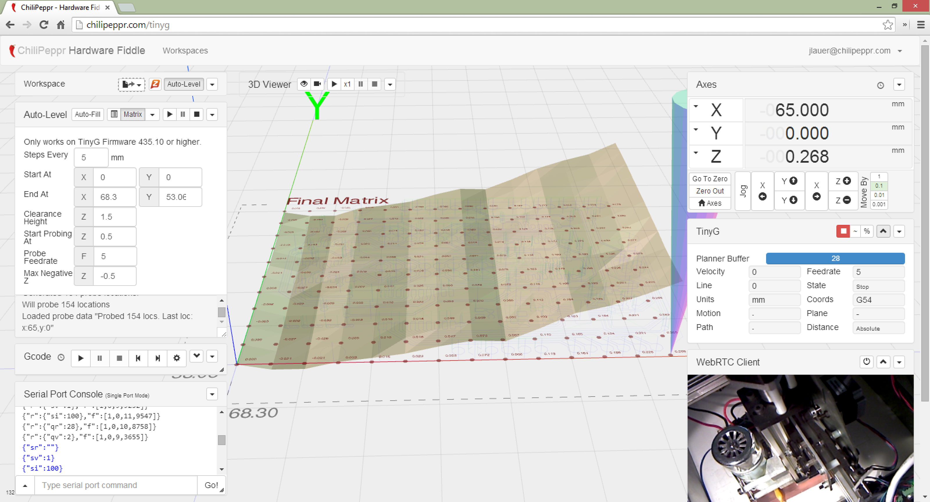
The results of the PCB auto-leveller in the image are exaggerated by 50x to help see the warpage. In the worst-case I have a 0.28mm rise from lower left to upper right. That’s a big deal which is exactly why I want to auto-level.
Question for you? How are you then converting your auto-level data to adjust Z-heights in your Gcode?
-
This reply was modified 12 years ago by
July 8, 2014 at 4:31 pm #6370MemberNice! And the PCB appears to be around 65 mm wide, so not big!
Question for you? How are you then converting your auto-level data to adjust Z-heights in your Gcode?
I don’t have a solution for that yet. I don’t have a height capture program either. Though the results you have seem to indicate it would indeed be worthwhile to implement it. I have some G-code manipulation code already written, but not this one..
I’ve actually been trying to make a two-sided 60 mm x 40 mm PCB with 0.2 mm isolation and 0.4 mm traces but so far I have failed. I think my problems would be solved if I were able to use cutting depth 0.05 mm, so 0.28 mm height variations would definitely kill that plan.
-
This reply was modified 12 years ago by
flux.
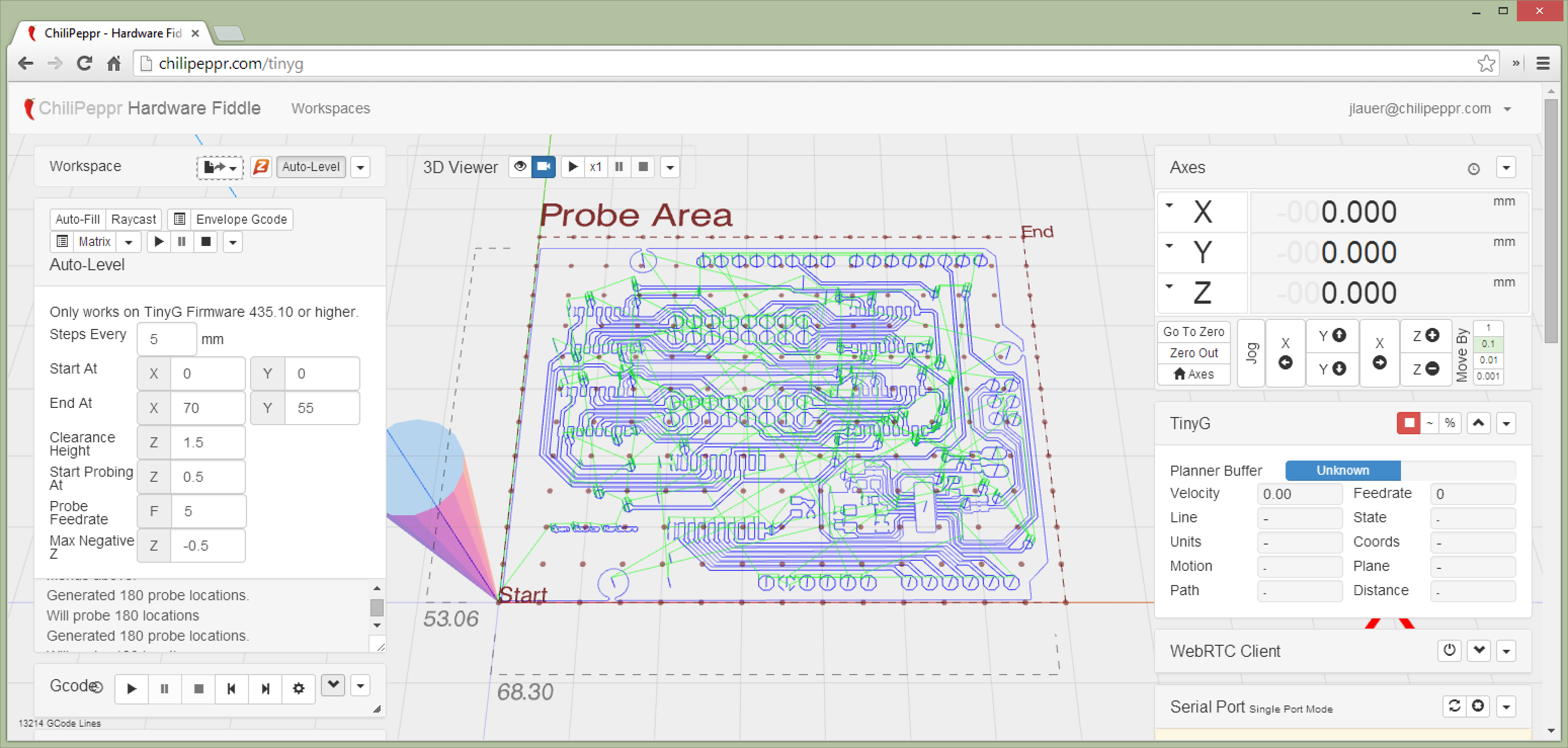
July 11, 2014 at 1:03 am #6395MemberOk, nailed it. I was able to use the Three.js library to do raycasting onto my mesh from the G38.2 command. That enables me to offset the Z. Here’s what it looks like.
At start of process you see region you’ll probe.
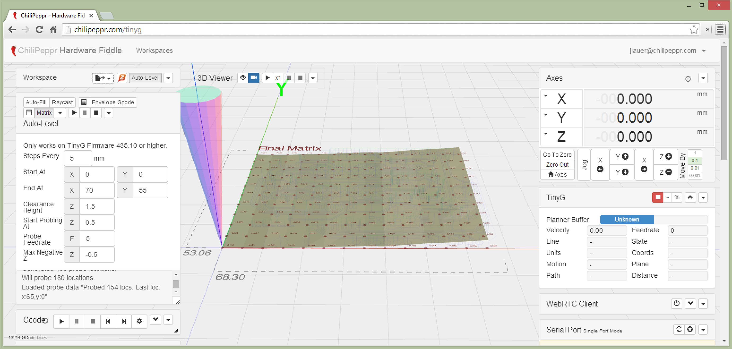
After probing you see your matrix. This is exaggerated 10x only.
Then you can view your raycasted PCB Gcode morphed to the probe data.
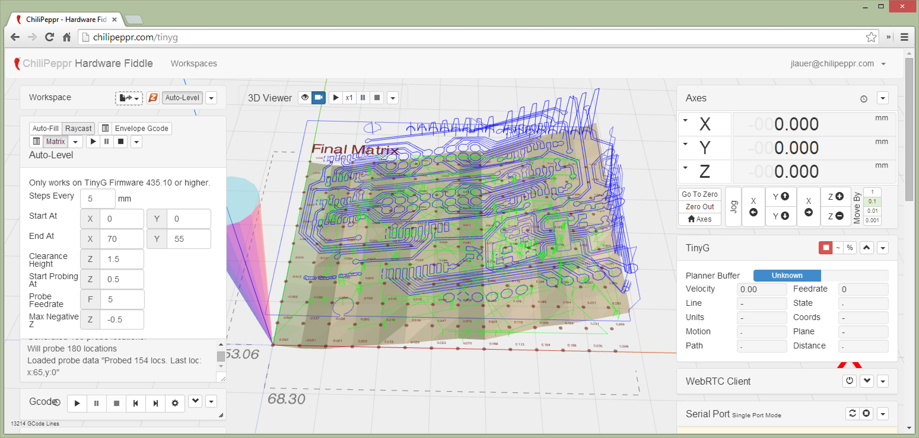
Then you get your final modified Gcode. Lines with Z’s get modified. Every G0/G1 without a Z gets a Z added to get best possible chance of matching probe warpage. Only problem remaining is splitting long G1 moves into sub-G1 moves to get better matching of warpage.
G00 Z2.0000 (al z mod 2) G00 X0.0000 Y0.0000 Z2.0000 (al new z) M03 G4 P3.000000 G00 X0.3147 Y0.3788 Z1.9983 (al new z) G01 Z-0.1017 F254.00 (al z mod -0.1) G01 X0.2800 Y0.4626 F508.00 Z-0.1015 (al new z) G01 X0.2800 Y52.8773 Z-0.1015 (al new z) G01 X0.3147 Y52.9612 Z-0.1015 (al new z) G01 X0.3788 Y53.0253 Z-0.1015 (al new z) G01 X0.4626 Y53.0600 Z-0.1015 (al new z) G01 X14.6826 Y53.0600 Z-0.1015 (al new z) G01 X14.7078 Y53.0495 Z-0.1015 (al new z) -
This reply was modified 12 years ago by
-
AuthorPosts
- You must be logged in to reply to this topic.